Mémoire de maîtrise de type recherche February 9, 2023 Collaboration avec l’Université Hassan II de Casablanca au Maroc « Identification rapide… More Research and Students February 1, 2023 Students working on hyperspectral measurements of an integrated quantum-well-based SPR biosensor.… More BioNanophotonics is one of the main axes of our research. February 1, 2018 Photo courtesy of La Tribune, Sherbrooke.… More Inside the Laboratory February 1, 2016 Advanced research infrastructure is used to design and carry out our… More February 1, 2016 Students discussing their projects with the visitors from the Canadian industrial… More Hard at Work February 1, 2015 Students discussing research in the laboratory.… More Orford, February 15, 2013 February 15, 2013 The QS Group Ski Day… More February 2, 2013 Miss Neng Liu at the Photonics West Conference, February 2-7, 2013,… More Professor Jian-Jun He, Zhejiang University, Hangzhou, China August 1, 2009 Visiting our laboratory in August 2009… More Bromont, winter 2009 February 1, 2009 The QS Group Ski Day at Bromont, February 2009.… More Professor Speaking September 9, 2008 Jan Dubowski speaking at the 6th International Conference on Photo-Excited Processes… More QS Group, August 2008 August 1, 2008 Alvaro Jimenez, Radoslaw Stanowski, Adnane Abdelghani (visiting professor), Alex Voznyy, Jan… More China 2008 February 1, 2008 Henry Helvajian, Jan Dubowski and Radoslaw Stanowski visiting the Great Wall… More Prof. John Polanyi (Nobel Prize Laureate) September 19, 2005 Prof. John Polanyi, delivers a lecture on “The Atomic Patterning of… More Employment 01 Mémoire de maîtrise de type recherche February 9, 2023 Collaboration avec l’Université Hassan II de Casablanca au Maroc… More Recent Publications 01 Walid M. Hassen, Jonathan Vermette, Houman Moteshareie, Azam F. Tayabali, Jan J. Dubowski, “Semi-automated water sampling module for repeated sampling and concentration of Bacillus cereus group spores”, Scientific Reports (Nature), 13:831 (2023). March 4, 2023 02 Houman Moteshareie, Walid M. Hassen, Yasmine Dirieh, Emma Groulx, Jan J. Dubowski, Azam F. Tayabali, “Rapid, Sensitive, and Selective Quantification of Bacillus cereus Spores Using xMAP Technology”, Microorganisms 10(7), 1408 (2022). March 4, 2023 03 Juliana Chawich, Walid M. Hassen, Amanpreet Singh, Daniela T. Marquez, Maria C. DeRosa, Jan J. Dubowski, “Polymer Brushes on GaAs and GaAs/AlGaAs Nanoheterostructures: A Promising Platform for Attractive Detection of Legionella pneumophila“, ACS Omega 7, 33349-33357 (2022). March 4, 2023 04 Lucas Paladines, Walid M. Hassen, Juliana Chawich, Stefan Dübel, Simon Lévesque, Jan J. Dubowski, Eric H. Frost, “Investigation of Conditions for Capture of Live Legionella pneumophila with Polyclonal and Recombinant Antibodies”, Biosensors 12, 380 (2022). March 4, 2023 News and Hot Stories Mémoire de maîtrise de type recherche Collaboration avec l’Université Hassan II de Casablanca au Maroc « Identification rapide des bactéries par ablation laser et spectroscopie infrarouge » Le projet vise à développer une… More February 9, 2023 MSc and PhD positions (Physics, Electrical Engineering, Biophysics) available from January 2019 MSc and PhD positions (Physics, Electrical Engineering, Biophysics) available from January 2019… More September 7, 2018 In situ Monitored Interaction Between Electrically Charged Molecules and Functionalized Surfaces of III-V Quantum Semiconductors (English, French) In situ Monitored Interaction Between Electrically Charged Molecules and Functionalized Surfaces of III-V Quantum Semiconductors (English, French)… More February 27, 2018 Digital Photo-Etching of III-V Semiconductors: Innovative Technology for Nanoscale Device Fabrication (English, French) Digital Photo-Etching of III-V Semiconductors: Innovative Technology for Nanoscale Device Fabrication (English, French)… More February 27, 2018 More News and Hot Stories ... Recently, We WEre There... 01 J.J. Dubowski, S. Aithal, N. Liu, H. Sharma, “Photoluminescence monitored photocorrosion for metrology of GaAs/AlGaAs heterostructures at the nanoscale” [Digital etching of GaAs: a 30-year (almost) perspective], an oral presentation at the Synthesis and Photonics of Nanoscale Materials XIV Symposium, SPIE Photonics West, San Francisco, USA, January 28 – February 2, 2017. February 27, 2018 02 W.M. Hassen, J.J. Dubowski, “Detecting Legionella pneumophila with Digitally Photocorroding Biosensor”, an oral presentation at the Biosensor Workshop on Detecting of Electrically Charged Biomolecules, Interdisciplinary Institute for technological Innovation (3IT), Université de Sherbrooke, Sherbrooke, Québec, November 15, 2017. November 15, 2017 03 M.R. Aziziyan, J.J. Dubowski, “Quantum Semiconductor Photonic Biosensing Platform for Detection of Legionella Pneumophila in Industrial Water”, an oral presentation at the 4th Student CRIBIQ (Consortium de recherche et innovation en bioprocédés industrielles au Québec) Symposium, Quebec City, September 25-26, 2017. September 26, 2017
Mémoire de maîtrise de type recherche February 9, 2023 Collaboration avec l’Université Hassan II de Casablanca au Maroc « Identification rapide… More
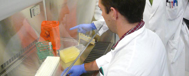
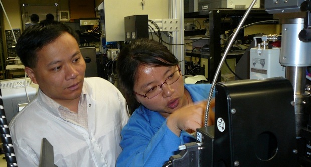
Research and Students February 1, 2023 Students working on hyperspectral measurements of an integrated quantum-well-based SPR biosensor.… More
BioNanophotonics is one of the main axes of our research. February 1, 2018 Photo courtesy of La Tribune, Sherbrooke.… More
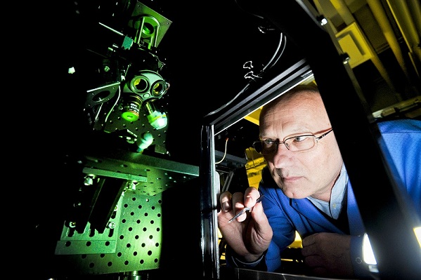
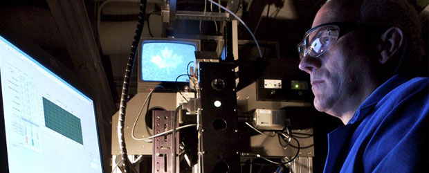
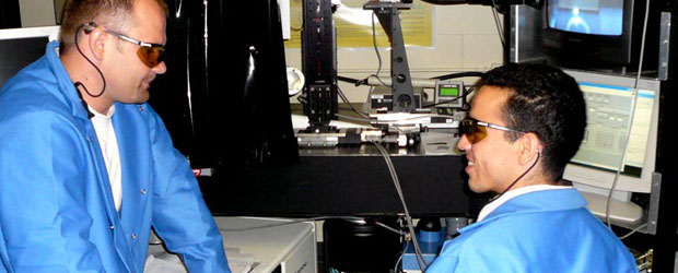
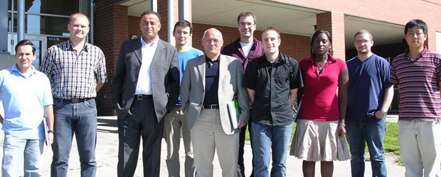
Inside the Laboratory February 1, 2016 Advanced research infrastructure is used to design and carry out our… More
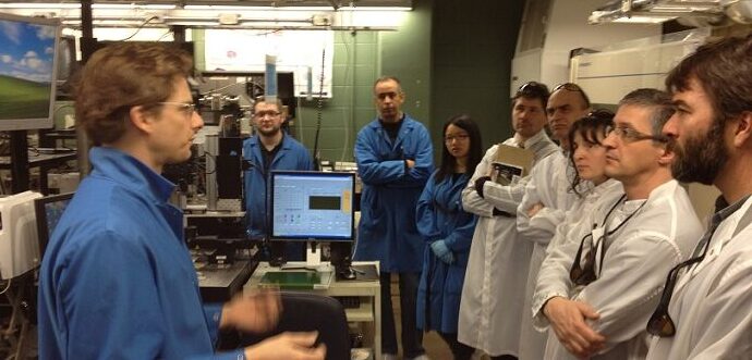
February 1, 2016 Students discussing their projects with the visitors from the Canadian industrial… More
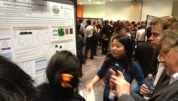
Professor Jian-Jun He, Zhejiang University, Hangzhou, China August 1, 2009 Visiting our laboratory in August 2009… More
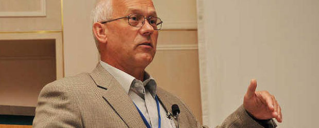
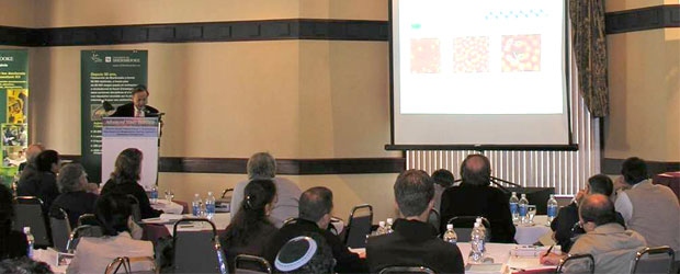
Professor Speaking September 9, 2008 Jan Dubowski speaking at the 6th International Conference on Photo-Excited Processes… More
QS Group, August 2008 August 1, 2008 Alvaro Jimenez, Radoslaw Stanowski, Adnane Abdelghani (visiting professor), Alex Voznyy, Jan… More
China 2008 February 1, 2008 Henry Helvajian, Jan Dubowski and Radoslaw Stanowski visiting the Great Wall… More
Prof. John Polanyi (Nobel Prize Laureate) September 19, 2005 Prof. John Polanyi, delivers a lecture on “The Atomic Patterning of… More
01 Mémoire de maîtrise de type recherche February 9, 2023 Collaboration avec l’Université Hassan II de Casablanca au Maroc… More
01 Walid M. Hassen, Jonathan Vermette, Houman Moteshareie, Azam F. Tayabali, Jan J. Dubowski, “Semi-automated water sampling module for repeated sampling and concentration of Bacillus cereus group spores”, Scientific Reports (Nature), 13:831 (2023). March 4, 2023
02 Houman Moteshareie, Walid M. Hassen, Yasmine Dirieh, Emma Groulx, Jan J. Dubowski, Azam F. Tayabali, “Rapid, Sensitive, and Selective Quantification of Bacillus cereus Spores Using xMAP Technology”, Microorganisms 10(7), 1408 (2022). March 4, 2023
03 Juliana Chawich, Walid M. Hassen, Amanpreet Singh, Daniela T. Marquez, Maria C. DeRosa, Jan J. Dubowski, “Polymer Brushes on GaAs and GaAs/AlGaAs Nanoheterostructures: A Promising Platform for Attractive Detection of Legionella pneumophila“, ACS Omega 7, 33349-33357 (2022). March 4, 2023
04 Lucas Paladines, Walid M. Hassen, Juliana Chawich, Stefan Dübel, Simon Lévesque, Jan J. Dubowski, Eric H. Frost, “Investigation of Conditions for Capture of Live Legionella pneumophila with Polyclonal and Recombinant Antibodies”, Biosensors 12, 380 (2022). March 4, 2023
Mémoire de maîtrise de type recherche Collaboration avec l’Université Hassan II de Casablanca au Maroc « Identification rapide des bactéries par ablation laser et spectroscopie infrarouge » Le projet vise à développer une… More February 9, 2023
MSc and PhD positions (Physics, Electrical Engineering, Biophysics) available from January 2019 MSc and PhD positions (Physics, Electrical Engineering, Biophysics) available from January 2019… More September 7, 2018
In situ Monitored Interaction Between Electrically Charged Molecules and Functionalized Surfaces of III-V Quantum Semiconductors (English, French) In situ Monitored Interaction Between Electrically Charged Molecules and Functionalized Surfaces of III-V Quantum Semiconductors (English, French)… More February 27, 2018
Digital Photo-Etching of III-V Semiconductors: Innovative Technology for Nanoscale Device Fabrication (English, French) Digital Photo-Etching of III-V Semiconductors: Innovative Technology for Nanoscale Device Fabrication (English, French)… More February 27, 2018
01 J.J. Dubowski, S. Aithal, N. Liu, H. Sharma, “Photoluminescence monitored photocorrosion for metrology of GaAs/AlGaAs heterostructures at the nanoscale” [Digital etching of GaAs: a 30-year (almost) perspective], an oral presentation at the Synthesis and Photonics of Nanoscale Materials XIV Symposium, SPIE Photonics West, San Francisco, USA, January 28 – February 2, 2017. February 27, 2018
02 W.M. Hassen, J.J. Dubowski, “Detecting Legionella pneumophila with Digitally Photocorroding Biosensor”, an oral presentation at the Biosensor Workshop on Detecting of Electrically Charged Biomolecules, Interdisciplinary Institute for technological Innovation (3IT), Université de Sherbrooke, Sherbrooke, Québec, November 15, 2017. November 15, 2017
03 M.R. Aziziyan, J.J. Dubowski, “Quantum Semiconductor Photonic Biosensing Platform for Detection of Legionella Pneumophila in Industrial Water”, an oral presentation at the 4th Student CRIBIQ (Consortium de recherche et innovation en bioprocédés industrielles au Québec) Symposium, Quebec City, September 25-26, 2017. September 26, 2017