Laser-induced bandgap engineering of III-V quantum semiconductors
The objective of this research is to investigate both fundamental and applied aspects of laser-based processes of quantum well and quantum dot intermixing that have the potential to lead to cost-attractive fabrication of advanced photonic devices or monolithically integrated photonic circuits that otherwise would have not been attainable with conventional micro-/nanofabrication methods.
Selective area bandgap engineering of quantum semiconductor heterostructures is the subject of intense investigation due to the potential of this approach in the fabrication of advanced devices and photonic integrated circuits (PICs). The challenge is to develop an innovative manufacturing technology capable of cost-attractive delivery of PICs. For quantum well (QW) and quantum dot (QD) microstructures, spatially selective intermixing of the QW (QD) and barrier material, known as quantum well (dot) intermixing (QWI/QDI), has been investigated as a feasible route to this end. The selective area intermixing and tuning of the QD emission wavelength is of particular interested due to the attractive perspective of applications of QDs as photon emitters, detectors and solar cells.

Figure 1. Photoluminescence map of an InGaAs/InGaAsP QW sample with an array of sites emitting at different wavelengths obtained with the UV-QWI technique [J. Genest, PhD thesis].
Lasers are highly attractive for the post-growth processing technologies due to the ease with which they can modify surface properties or temperature of wafers in selected sites. The success of such an approach will depend on the progress of our understanding of the fundamental phenomena governing the laser-matter interaction. At the UdeS Laboratory for Quantum Semiconductors and Laser-based Nanotechnology, we investigate QW/QD intermixing phenomena using UV excimer lasers (UV-QWI) and an IR Laser-RTA (rapid thermal annealing) technique. Figure 1 shows an example of an InGaAs/InGaAsP QW sample that following selective area irradiation with a 193 nm excimer laser was annealed at 725 °C for 120 sec. Blue-shifts in excess of 100 nm can easily be achieved for such QW microstructures.
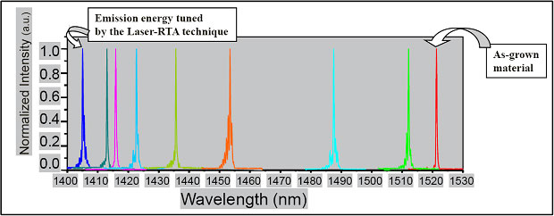
Figure 2. Emission spectra from a monolithically integrated (2 mm long) multi-wavelength semiconductor laser chip obtained with the Laser-RTA technique.
Figure 2 shows a series of emission spectra obtained from a monolithically integrated multiwavelength laser chip fabricated with the Laser-RTA technique. A modeling study has indicated that the Laser-RTA technique has the potential to provide significant blue shifts with micrometer-size spatial resolution. Thus, this one-step post-growth processing approach is particularly attractive for tuning emission wavelength of individual QDs or their ensembles grown on nano-patterned substrates. The Laser-RTA technique is investigated with a variety of CW laser sources (405, 473, 532, 980, 1064 and 10600 nm) which, depending on a studied QW/QD heterostructure, are used individually or in tandems.
- G. Genest, J.J. Dubowski and V. Aimez, “Suppressed intermixing in InAlGaAs/AlGaAs/GaAs and AlGaAs/GaAs quantum well heterostructures irradiated with a KrF excimer laser”, Appl. Phys. A89, 423-426 (2007).
- O. Voznyy, R. Stanowski and J.J. Dubowski, “Multibandgap quantum well wafers by IR laser quantum well intermixing: simulation of the lateral resolution of the process”, J. Laser Micro/Nanoengineering, 1(1), 48-53 (2006).
- J.J. Dubowski, C.Y. Song, J. Lefebvre, Z. Wasilewski, G. Ares and H.C. Liu, “Laser-induced selective area tuning of GaAs/AlGaAs quantum well microstructures for two color IR detector operation”, J. Vac. Sci. Tech. A22(3), 887-890 (2004).